The right climate for efficient semiconductors
Electrical Terms
💫 What do the terms bandgap, diode, kilohertz, semiconductor, substrate and transistor mean?
- Bandgap – a measure of the energy that must be given to an electron so that it can contribute to electrical conduction between the valence band and the conduction band of a solid material (such as an insulator or semiconductor).
- Diode – a semiconductor device with two terminals that enables flow of current in one direction only.
- Kilohertz – a switching frequency of one thousand times per second.
- Semiconductor – a solid substance that conducts between an insulator and most metals. Its conductivity changes with the addition of an impurity or temperature. Devices made of semiconductors are essential components of most electronic circuits.
- Substrate – an underlying substance or layer for depositing semiconducting films.
- Transistor – a device that is used to amplify or switch electronic signals and electrical power.
Average global temperatures are rising, with the worst-case scenario having devastating implications. Humans are encouraged to make changes to their lifestyles to try to curb the heating of our planet. Some options are not going to be universally popular, as many of us enjoy tucking into a steak, holidaying on different continents, and taking the car rather than the bus.
However, there is one change that could be easier to implement and be done without the average person even knowing: moving to greater efficiencies for the conversion of electricity every time it changes from one form to another. For example, converting between alternating and direct currents (AC and DC), changing the voltage or frequency, or a combination of these. Power conversion is inherent in the electrical systems of many products, from high-speed bullet trains and electric cars to laboratory equipment and solar panels, but energy is often wasted during the process.
Power conversion is inherent in the electrical systems of many products, from high-speed bullet trains and electric cars to laboratory equipment and solar panels, but energy is often wasted during the process
The simplest way to increase efficiency and reduce losses during electricity conversion is to improve the prevailing technology: silicon power devices. However, these devices have been refined over many years, and it would take significant effort and scientific breakthroughs to deliver even a modest gain to the efficiency of the key components: the diodes, which block current in one direction, while allowing it to pass in the other; and the transistors, the switches that turn the current off and on.
A far more promising approach is to develop diodes and transistors from semiconductor materials with superior attributes, such as silicon carbide (SiC), gallium nitride (GaN) and gallium oxide (Ga2O3). The gains in efficiency are so significant that leading silicon device manufacturers have been investing in alternatives for several years. While sales of silicon still dwarf the alternatives, shipments of devices made from SiC are well established and rising rapidly. According to French market analyst Yole Développement, revenue for SiC power electronics hit $460 million in 2018 and will rocket to $1.5 billion by 2023.
The advantages that SiC has over silicon stem from the far higher value of its bandgap. Excellent electrical conductors, such as metals, have a bandgap that is zero, while insulators, which do not conduct, have an incredibly high bandgap. In general, the wider the bandgap, the more efficient the power conversion.
In general, the wider the bandgap, the more efficient the power conversion.
Thanks to its higher bandgap, a SiC device that is as thick as one made of silicon can block a far higher voltage. Alternatively, a far thinner device can block the same voltage, while reducing the distance that current must flow. This cuts resistance, creating more efficient devices with lower losses.
Another merit of SiC devices is that they can turn on and off more quickly than those made from silicon, so waste less energy when switching. This strength is highly valued in modern electrical circuits used to either convert signals between AC and DC forms, or step up or down voltages, as this is often carried out by switching currents on and off at frequencies of tens of kilohertz or more.
The significant energy savings associated with the more abrupt switching of SiC, allied to its lower resistance, are highlighted in comparisons of circuits equipped with these devices and those sporting only silicon electronics. For example, measurements by the Fraunhofer Institute for Solar Energy Systems show that replacing a silicon transistor with one made with SiC propels the efficiency of an inverter (a device that converts DC to AC) from just over 97% to a figure 1.6% higher. To look at it another way, losses are more than halved.
While such gains in efficiency may not appear to be that substantial, they can be if SiC is widely deployed. Suppose, for example, that the energy saving of 1.6% is applied to global electricity production, which totalled nearly 21,000 terawatt-hours in 2016, according to International Energy Agency statistics. This would equate to a saving of 340 terawatt-hours, which is close to the total annual electricity generation of the UK.
This would equate to a saving of 340 terawatt-hours, which is close to the total annual electricity generation of the UK
From a user’s perspective, there can be an even bigger benefit than an increase in efficiency when moving to SiC devices: a reduction in the size, weight and cost of the electrical unit. As SiC devices can turn on and off far faster than those made from silicon, circuits are not limited to switching frequencies of typically tens of kilohertz. Hundreds of kilohertz are possible and this allows the use of far smaller, lighter and cheaper inductors and capacitors.
Delivering the diode
In 2001, semiconductor manufacturer Infineon Technologies pioneered the first commercial SiC product with its SiC Schottky barrier diode, a device capable of blocking 600 volts. The SiC Schottky barrier diode, the simplest possible diode, is made by depositing a thin semiconducting film on a substrate, which is a thin, circular disc that provides a foundation for the device. After this, engineers process the coated substrate into thousands of chips, and on each one they add a metal contact to the front and back.

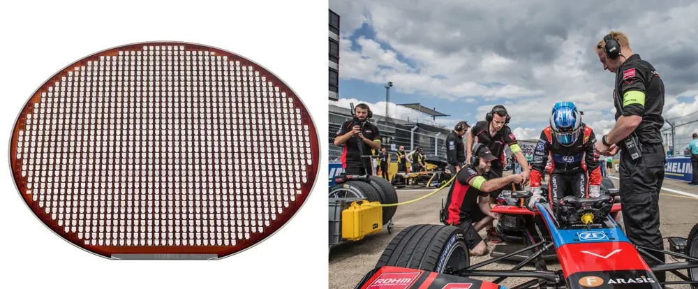
A SiC wafer with MOSFETs, such as those that are paired with diodes and used in the electrical systems of some Formula E racing cars © Infineon Technologies (left), Rohm (right)
Such simple architecture cannot handle high-current pulses experienced in the field, so a far more complex design has replaced it. Further refinements have followed and today Infineon offers sixth-generation products for power supplies, as well as fifth-generation cousins for other applications. The voltage range has also expanded to include diodes with a 1.2 kV (kilovolts) blocking voltage.
When Infineon started manufacturing its diodes, substrates were just 50 millimetres in diameter. Back then, the company produced silicon devices on 125 millimetre or 150 millimetre substrates, making its production equipment ill-suited to making SiC devices.
SiC substrates have come a long way since then. They are now available in diameters up to 150 millimetres and the quality is far better, with the device-killing defects that plagued initial generations largely eradicated.
SiC Schottky barrier diodes and MOSFETS
⚛️ p-type materials, n-type materials and holes to control current flow
The simple architecture of a Schottky barrier diode is formed by sandwiching a film of semiconducting material between two metal contacts. When made of SiC, it can block hundreds of volts when a negative voltage is applied and conduct electricity with low resistance when a small positive voltage is applied.
The SiC film that lies at the heart of the device has a crystalline structure. This hampers current flow, because the four electrons in the outer shell of every carbon and silicon atom form strong covalent bonds and are not free to move. Therefore, to boost the current, engineers intentionally add a carefully chosen impurity – a material with a fifth electron in its outer shell. As this fifth electron is free to roam, it enhances electrical conductivity, thereby trimming resistance.
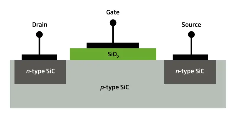
Material with this characteristic is known as n-type, because of the negative charges, and is used in the most common form of SiC transistor, the SiC MOSFET. In this device, a voltage is applied between the source and drain contacts, which are both connected to n-type regions of material. Separating these regions is p-type material, formed by adding an intentional impurity with just three electrons in its outer shell. As four electrons from each atom are needed for bonding, there is an absence known as a hole. It spreads through the material, acting as a positive charge carrier. Applying a positive voltage to the gate drives away the holes beneath this region, creating an n-type channel just below the surface of the silicon dioxide (SiO2) insulating layer. This channel allows a large current to flow when a voltage is applied between the source and drain. Removing the voltage causes the current to stop.

Targeting the transistor
After the launch of the SiC diode, the race was on to make a commercial transistor with this material. By 2008, the first products hit the market but sales failed to take off.
According to Hong Lin, a senior technology and market analyst at Yole Développement, the first products were held back by the improvements made to their silicon rivals and, in general, circuit designers did not want to work with such a different product.
It took three more years before the market had a drop-in replacement for the silicon transistor: US-based company Wolfspeed’s SiC, metal-oxide semiconductor field-effect transistor (MOSFET). This features a silicon dioxide insulating layer between the SiC film and the metal contact. Getting this device to market was a struggle: it took many years to remove the imperfections in the oxide layer so that current could flow freely.
Today, several companies manufacture SiC MOSFETs. Japanese company Rohm, which released its device just after Wolfspeed, is pairing it with a diode in an SiC module used in the systems of electric racing cars made by Venturi, a competitor in Formula E. Meanwhile, Mitsubishi’s SiC MOSFETs are used in Japan’s electric trains, and STMicrolectronics’ variants are going in the all-electric Model 3 Tesla.
One factor behind the recent success is the greater availability of 150 millimetre substrates that cut production costs, creating what Peter Friedrichs, Senior Director of SiC at Infineon Technologies, describes as a ‘tipping point’ in the market. In his opinion, the superior performance of SiC in some applications compensates for the higher cost.
Fuelling this growth in sales are the increasing use of solar power at high voltages and the roll out of fast chargers for electric vehicles. For both these applications it takes very little time to repay the additional expense associated with SiC devices.
Superiority stems from the bandgap
🗲 How the bandgap and thermal conductivity can govern the performance of electronic devices
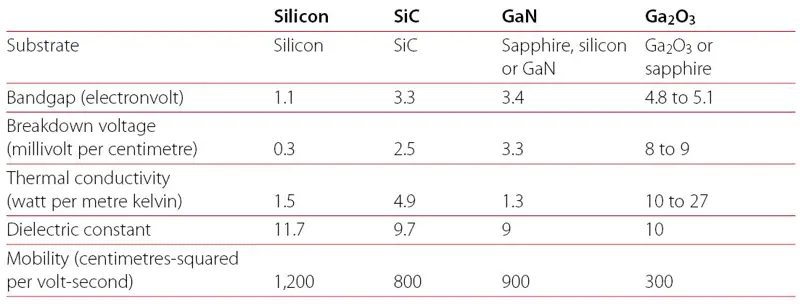
Bandgap governs the performance of semiconductor power electronics devices. In general, if a material has a higher bandgap, it will have a higher breakdown voltage and can be used in devices that operate at a higher voltage – or one that uses less material while handling the same voltage as a lower-bandgap equivalent.
Another important property is the thermal conductivity. For SiC, it is more than three times that of silicon and GaN, but much less than that for gallium oxide. A high thermal conductivity is a valuable asset as it increases the capability of a device to reduce temperature and thus run at a lower temperature. When SiC devices replace those made from silicon, this may go hand-in-hand with the removal of cooling units for the device, trimming cost, space and weight.

Bandgap values for common materials
The growth of gallium nitride
GaN, which is used to make the LEDs that backlight device screens and increase the efficiency and lifetime of lightbulbs, has a similar bandgap to SiC. Its diodes and transistors work at lower voltages, such as 600 volts and below. As this market is bigger than that for higher voltages, where SiC serves, sales of GaN devices could eventually eclipse those of SiC. Today, however, annual revenue is only around $10 million, with devices used in power supplies in data centres and consumer applications.
Ideally, GaN devices would be made on GaN substrates, but this foundation is expensive and limited in availability, so silicon substrates are often used. This results in complications because the spacing of atoms in the silicon crystal differs from that in GaN. This mismatch causes strain to build up when growing a film of GaN on silicon, giving rise to imperfections that impair device performance. The trick is to trap these imperfections in a layer close to the substrate, before growing a device with high material quality on top.

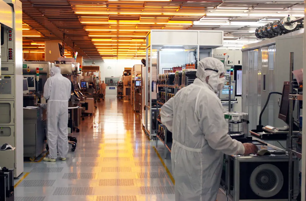
Newport Wafer Fab is at the heart of a UK cluster that is developing GaN semiconductor devices and processes © Newport Wafer Fab
Efforts to perfect this approach are well rewarded. It is not just that silicon substrates are far cheaper than both GaN and SiC, and more widely available in diameters of up to 300 millimetres. It is also that the GaN-on-silicon wafers can be processed relatively cheaply, and easily, in silicon fabrication plants (also known as fabs).
A team of engineers from Newport, South Wales, pioneered the GaN-on-silicon transistor. The Newport Wafer Fab team works at a foundry once owned by power semiconductor specialist International Rectifier, which used to develop GaN transistors from 2009. Device production then involved the growth of GaN layers on silicon at an external foundry in Minnesota, followed by the processing of this material into transistors at the fabrication plant in South Wales. Products were shipped to audio equipment manufacturers to use in high-end amplifiers.
In 2015, Infineon bought International Rectifier for $3 billion. After evaluating its global foundry capabilities, Infineon decided to sell the Newport facility. This led to the launch of the Newport Wafer Fab, which processes coated substrates into devices on behalf of other companies. Newport Wafer Fab now plays a very active role in a regional cluster developing new GaN semiconductor devices and processes. At nearby Swansea University, researchers are developing processes to make GaN power electronics to create a technology that is available to those that partner with the Newport plant.
The promise of Gallium Oxide
Offering even greater efficiencies than SiC and GaN is Ga2O3, a material with a bandgap that is about 50% higher. A leading developer of these devices is Japanese company Flosfia, which is pioneering a novel growth technology to deposit films of this oxide on sapphire substrates, the most common platform for LED production. Initial results for diodes and transistors are very encouraging, including a new benchmark for resistance. Mass production of diodes will begin later this year, with the addition of MOSFETs slated for 2021. However, Lin believes it will be some time until these devices have significant commercial success.
UK: Supporting production
👩🏭 The role of UK companies in the global wide-bandgap power electronics industry
UK companies are playing a significant role in the global wide-bandgap power electronics industry. The UK does not have a device maker, but has a foundry offering the processing of SiC material into diodes and transistors, and two companies making tools for the production of GaN and SiC devices.
Clas-SiC Wafer Fab in Lochnelly, Scotland, offers foundry services for producing devices from substrates coated with SiC films. This startup, led by engineers that gained valuable experience in SiC while working at Raytheon Systems’ facility in Glenrothes, can turn a customer’s design for a diode into a working device within four weeks, with an eight-week turnaround for a transistor.
The equipment at Clas-SiC can process 150-millimetre diameter material, the preferred size for the SiC industry. The facility can be used for small-volume, rapid prototyping, and production up to what is described as ‘medium volumes’.
Production of SiC devices can involve the etching of trenches to define the device architecture. Processing equipment made by SPTS Technologies is capable of uniform vertical and tapered etches and can feature optical instruments to measure the depth of the trench during the etching process.
GaN devices grown on silicon may require the etching of holes through the entire structure, including the substrate or gently through GaN layers. SPTS’s equipment can etch silicon at high speeds and provide slower, low-damage etching of GaN.
Oxford Instruments Plasma Technology, based in Yatton, has more than 30 years’ experience in developing plasma deposition and etching technologies to produce various semiconductor devices. One of its great strengths, highly valued by the manufacturers of SiC and GaN devices, is producing processing equipment that can either remove or deposit material one atomic layer at a time. With this approach, when material is removed, damage to sensitive layers is minimised, ensuring high-performance devices. When material is added, such as when an aluminium oxide insulator is deposited, it is done so with tremendous accuracy, fine tuning the device’s electrical properties.
Enhanced efficiency
Devices made from these wide-bandgap semiconductors are taking significant market share from silicon devices, as engineers are moving away from using silicon. As well as the efficiency gains, the materials can operate at higher frequencies so other components can be smaller, which also leads to savings in size, weight and cost of electrical systems.
Every time you surf the internet, devices with wide bandgaps decrease the energy consumed by the server farms
Every time you surf the internet, devices with wide bandgaps decrease the energy consumed by the server farms. When you buy an electric car, they are likely to lie at the heart of the electronics that power both it and the accompanying, growing network of fast-charging stations. Factor in the use of SiC in trains, the electrical grid, and solar and wind farms, and it’s easy to see why these alternatives to silicon are going to play an ever-increasing role in electrical and electronic engineering.
***
This article has been adapted from "The right climate for efficient semiconductors", which originally appeared in the print edition of Ingenia 78 (March 2019).
Keep up-to-date with Ingenia for free
SubscribeRelated content
Electricals & electronics

Accelerometers
Used in earthquake measurements, laptops, planes and even in stargazing apps, today’s accelerometers are much smaller than when they were first developed in 1927. Find out how they detect movement and vibration.

How to maximise loudspeaker quality
Ingenia asked Dr Jack Oclee-Brown, Head of Acoustics at KEF Audio, to outline the considerations that audio engineers need to make when developing high-quality speakers.

Cable fault locator
The winner of the Institute of Engineering and Technology’s 2014 Innovation Award was EA Technology’s CableSnifferTM, which uses a probe and chemical sensing technology to identify faults, saving energy companies millions of pounds each year.

High speed evolution
In December 2010, Eurostar International Ltd awarded a contract for 10 new high speed trains to Siemens. The company has used a system developed over decades to maximise the performance and passenger-carrying ability of its 320km/h trains.
Other content from Ingenia
Quick read

- Environment & sustainability
- Opinion
A young engineer’s perspective on the good, the bad and the ugly of COP27

- Environment & sustainability
- Issue 95
How do we pay for net zero technologies?
Quick read

- Transport
- Mechanical
- How I got here
Electrifying trains and STEMAZING outreach

- Civil & structural
- Environment & sustainability
- Issue 95