Metamaterials, metalenses and beyond
Did you know?
📱 Metalenses in modern technology
- Most current smartphones have a stack of six or seven lenses in their cameras
- Metalenses can be 100x thinner than a human hair, and focus light with nanopillars rather than curved glass
- They could replace stacks of lenses in current cameras and even help us see smaller than the diffraction limit of light 📷
Made from volcanic glass, the first known artificial mirrors date back 8,000 years; while Egyptian hieroglyphs suggest that lenses were already used in ancient Egypt. One of the earliest known lenses, made in about 750 to 710BCE, is a polished quartz crystal that may have been used as a magnifying glass. A few hundred years later, Greek writers reference burning glasses used to make fire – to the detriment of enemy ships if Archimedes is to be believed. The Roman Emperor Nero was even said to have used a concave emerald to watch the gladiators (thought to be for correcting near-sightedness or perhaps a kind of sunglass).
Optical technologies have clearly come a long way since then. Today, lenses can be mass manufactured and precisely shaped to fit any number of functions, whether it’s capturing macro images on a smartphone, observing the very large or very small with telescopes and microscopes, or simply correcting astigmatism. But despite this huge progress in optical engineering, the basic principles have remained the same.
Modern optical technology – such as cameras, microscopes, or telescopes – is still largely based on lenses and mirrors, and this is key in determining their size and weight. Indeed, the ever-decreasing thickness of the modern smartphone is partially determined by the thickness of the stack of lenses within its camera. This is the reason for the so-called ‘camera bump’ on most phones – where the lens of the camera protrudes beyond the flat body of the phone.
About two decades ago, early research into metamaterials began. These materials have unusual properties not found in nature, thanks to the shape, symmetry and composition of their nanoscale building blocks. Now, the same nanofabrication techniques that have enabled manufacturers to pack increasingly more transistors onto computer chips are being explored to make metamaterials with exciting optical properties. Not only could these make smartphones and cameras even more compact – they could also bring new kinds of sensing out of the lab and into entirely new places.
How structural features can change metamaterial properties
The optical properties of materials are controlled by their structure on the sub-wavelength scale. For light, with wavelengths of hundreds of nanometres (nm) – billionths of a metre – this is the arrangement of atoms, molecules, and the repeating lattice structure of crystals. Structural features this size interact with light in unique ways. For example, calcite’s crystal lattice produces birefringent properties, meaning that it doubly refracts light (which creates a double image of objects seen through the transparent crystal). A Christmas-tree-like nanostructure is why the Morpho butterfly’s wings appear so vividly blue, as light diffracts on the nanotrees and interferes.

(Main image) The Morpho butterfly’s iridescent blue wings are made up of thousands of scales © Unsplash. (Inset) The Christmas-tree-like nanostructures, seen here through a scanning electron microscope, are responsible for its vivid colour because of the way they interact with light © Shinya Yoshioka, Osaka University
What is a controllable metamaterial?
⚡ Changing optical properties with electricity
A controllable metamaterial is an artificial metamaterial that can be reconfigured to control its properties in specific areas.
When an electrical current is applied to an individual nanowire (zig-zag-shape), the nanowire is heated, thermally expands and is displaced. This change in the metamaterial’s structure on the nanoscale results in a change of its optical properties.
Using nanofabrication to engineer the structure of materials on this scale allows us to make metamaterials. When metamaterials emerged at the beginning of the 21st century, initial excitement was driven by the opportunity to engineer exotic properties: in particular, cloaking materials, and zero and negative refractive index materials. Cloaking materials have received much fanfare in the press as a way to make an object invisible by guiding light around it to hide it from view. Meanwhile, zero refractive index materials can be used to enhance nonlinear optical effects, for example to make artificial materials that can efficiently change the colour of light. On the other hand, a material with a refractive index of −1 could be used to make a perfect lens (with infinite resolution).
Arranging the same nanoscale components in different ways can result in drastic changes in a material’s properties. This can be easily understood by considering carbon atoms, which can form the soft, black graphite found in pencils, or brilliant, transparent, and hard diamond (not to mention fullerenes, graphene, and carbon nanotubes, which all have radically different properties again).
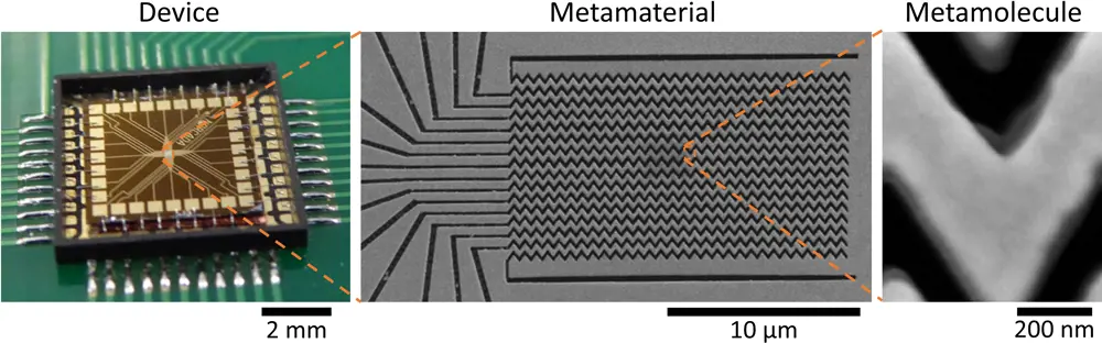
This 100 nanometre-thick metamaterial, made from gold on silicon nitride, was made using focused ion beam milling at the University of Southampton. © Nanophotonics & Metamaterials Group, University of Southampton
Metamaterials consist of metamolecules, which may be reconfigured to change the metamaterial’s properties. ‘Controllable metamaterial’ (above) shows an example of a device in which individual nanowires can be moved independently by electrical currents. Although the device shown is a proof of principle, with careful engineering, similar metamaterial devices could be used as spatial light modulators (like those that manipulate light in projectors) for creating holographic videos. Structures like this have been shown to respond to temperature, electric or magnetic fields, sound, and even light. This provides an opportunity to develop smart materials and sensors typical for applications like magnetic field sensing or radiation detection with very high spatial resolution.
Structures like this have been shown to respond to temperature, electric or magnetic fields, sound, and even light. This provides an opportunity to develop smart materials and sensors typical for applications like magnetic field sensing or radiation detection with very high spatial resolution.
How does it work?
🔎A comparison of light interaction with conventional lenses and metalenses
Slowing down light:
- A convex focusing glass lens slows down light for longer at its centre (the more glass, the more delay), than at its edges, bending the wavefronts of the light towards a focal spot. A large-diameter lens that focuses light strongly must be thick as it needs to delay light a lot at its centre.
- In contrast, a metalens uses nanostructures that reradiate the incident light with the right delay. Thanks to the nanostructures, the thickness of the lens is less than 1 micrometre. For comparison, a human hair is typically 70 micrometres thick.
Making lenses on the microscale
Today however, the metamaterials advance that’s on the brink of making a commercial impact is the metalens, which could transform the size, weight and complexity of optical systems. If cameras and phones are to continue on their trajectory of miniaturisation, conventional glass or plastic lenses won’t cut it. As illustrated in the ‘Slowing down light’ figure (right), these refractive lenses work by slowing down and therefore bending wavefronts of light, which requires them to be thick in certain regions.
Shrinking a lens down to an essentially flat surface requires a different approach. In a typical metalens, a surface (such as a flat, ultrathin piece of glass) is covered in nanoscale pillars. The size of the pillar determines how much it will delay light. To be able to delay the light field efficiently, the pillars need to be made from a material with a high refractive index, while low absorption is needed to make a transparent lens. Typical metalenses for visible light use titanium dioxide (widely used as white pigment) or gallium nitrude (used in LEDs) and metalenses for infrared light use silicon (used in electronics).
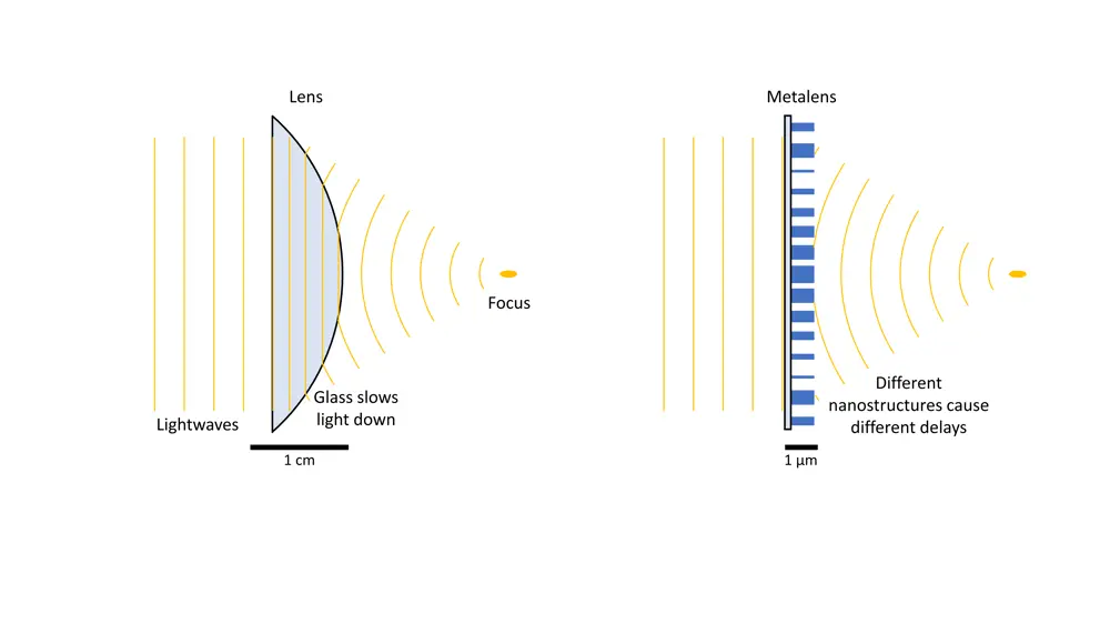
Slowing down light: Light waves interacting with a conventional lens (left) are slowed down depending on the thickness of the glass, whereas with a metalens (right), different nanostructures reradiate the incident light resulting in different delays © University of Southampton
How are metalenses made?
🧪Electron beam lithography
Metalenses can be prototyped using electron beam lithography, which offers the flexibility to try many different designs:
1. A beam of electrons exposes a layer of resist where pillars should be formed.
2. The exposed resist is washed away.
3. The pillar material is deposited with sufficient thickness to fill all the gaps and produce a flat surface.
4. Excess pillar material is etched away.
5. The remaining resist is removed and the metalens remains.
Metalenses can be mass produced by either using the pillars as a stamp (called nanoimprint lithography) or by replacing the first step with deep-UV lithography, for example by STMicroelectronics (Crolles, France).
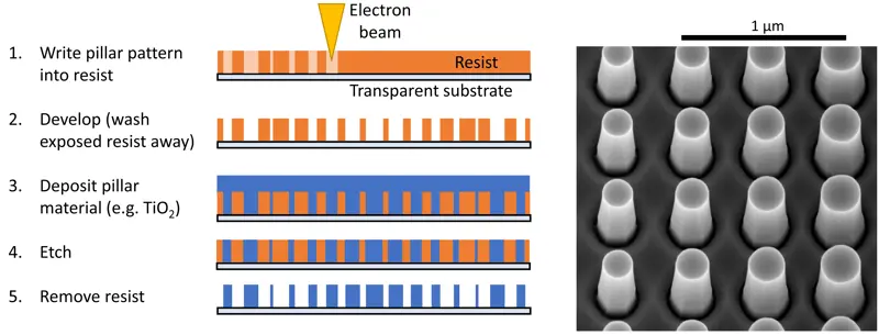
(Left) the process of electron beam lithography. (Right) gallium nitride pillars made by electron beam lithography at Kelvin Nanotechnology (Glasgow).
This means that just like a conventional lens, a nanostructured film less than a micrometre thick can direct light into a focal spot on an image sensor. It can even be used to generate a hologram with any desired distribution of light, for example, as a security feature for bank notes or passports. But while conventional lenses are made by moulding and polishing glass or plastic, metalenses and metamaterials can be made with the same manufacturing techniques as the semiconductor industry uses to make computer chips. Prototypes can be made using electron beam lithography, while deep-UV lithography provides a cost-effective solution for mass production of thousands of lenses in parallel.
However, a metalens can be more than an extremely thin and light version of a conventional lens. With the right nanostructure engineering, the shortcomings of normal glass lenses can also be avoided. These shortcomings are why a stack of six or seven conventional lenses is required in a state-of-the-art mobile phone camera: to compensate distortions and aberrations. Metalenses promise not just thinner lenses, but also fewer of them, which could spell the end of the camera bump. They might also surpass the image quality of today’s cameras with sharper, brighter images.
Overcoming the diffraction limit to zoom in on viruses
Another major challenge for conventional lenses is resolution. Much of our understanding of the biological world is based on what we can see through optical microscopes. Conventional lenses can focus light to a spot that is approximately half a wavelength in size, which is about 250 nm for visible light.
This so-called ‘diffraction limit’ is what prevents us from seeing viruses and proteins using light microscopes, as the resolution isn’t high enough. Focusing light into smaller spots is the key for seeing these smaller objects. (Other imaging techniques allow imaging of things this size, but samples must undergo harsh treatments such as being crystallised or cryogenically frozen. One example is electron microscopy, as seen in images in this article, which requires samples to be placed in a vacuum.)
Much of our understanding of the biological world is based on what we can see through optical microscopes.
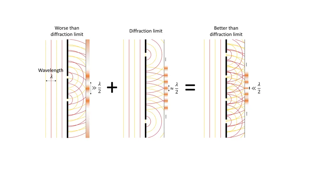
Beating the diffraction limit
🔬 The physics of diffraction limits
Waves have alternating crests (yellow) and troughs (red) that repeat after a distance known as wavelength λ. Light waves consist of an oscillating electric (and magnetic) field, with crests and troughs corresponding to the largest field in opposite directions. If light waves pass through a pair of slits, they will form a series of dark lines (crest meets trough, white) and bright lines (crests or troughs meet, orange). The lines become narrower as the slits are moved further apart until they reach a minimum width of half a wavelength: the diffraction limit. Smaller, indeed arbitrarily small, lines or focal spots may be achieved by combining several pairs of slits.
Fortunately, metalenses may be engineered to circumvent the diffraction limit, enabling light – or any other wave – to be concentrated in much smaller spots. The key to beating the diffraction limit is a concept known as superoscillations. The sum of slowly oscillating waves can have features that oscillate fast. ‘Beating the diffraction limit’ shows an example. Careful engineering of such structures allows light to be concentrated into lines or spots of much smaller size.
Light waves passing through slits in a screen, forming an interference pattern of bright and dark lines. The lines generated by a pair of slits have a width of at least half of the wavelength. However, if we combine pairs of slits, the superposition of the light fields can have much smaller features © University of Southampton
The final figure shows a superlens consisting of concentric ring slits in an aluminium film, which concentrates red light into a spot of less than 200 nm diameter. The price to pay is that tiny focal spots will only contain some of the incident light, but that has not prevented the development of super resolution microscopy far beyond the diffraction limit, for biology and beyond. Indeed, recent experiments at the Nanyang Technological University (Singapore) and at the University of Southampton demonstrate that tiny superoscillations can be used to create an ‘optical ruler’ that detects movements as small as 1 nm, corresponding to a resolution of λ/800 (where lambda, λ, is the wavelength). This indicates even atomic-scale resolution may be within reach.
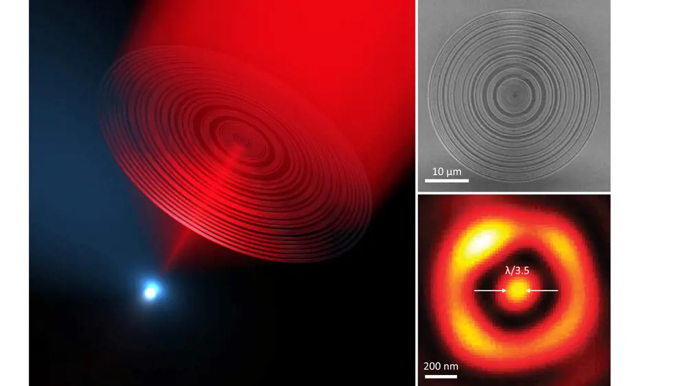
(Left) Artistic impression of a superoscillatory lens focusing light. (Top right) SEM image of a superoscillatory lens consisting of many circular slits in an aluminium film; (bottom right) the focal spot of 185 nanometres diameter that it produces when illuminated by red light of wavelength λ=640 nanometres © Nanophotonics & Metamaterials Group, University of Southampton
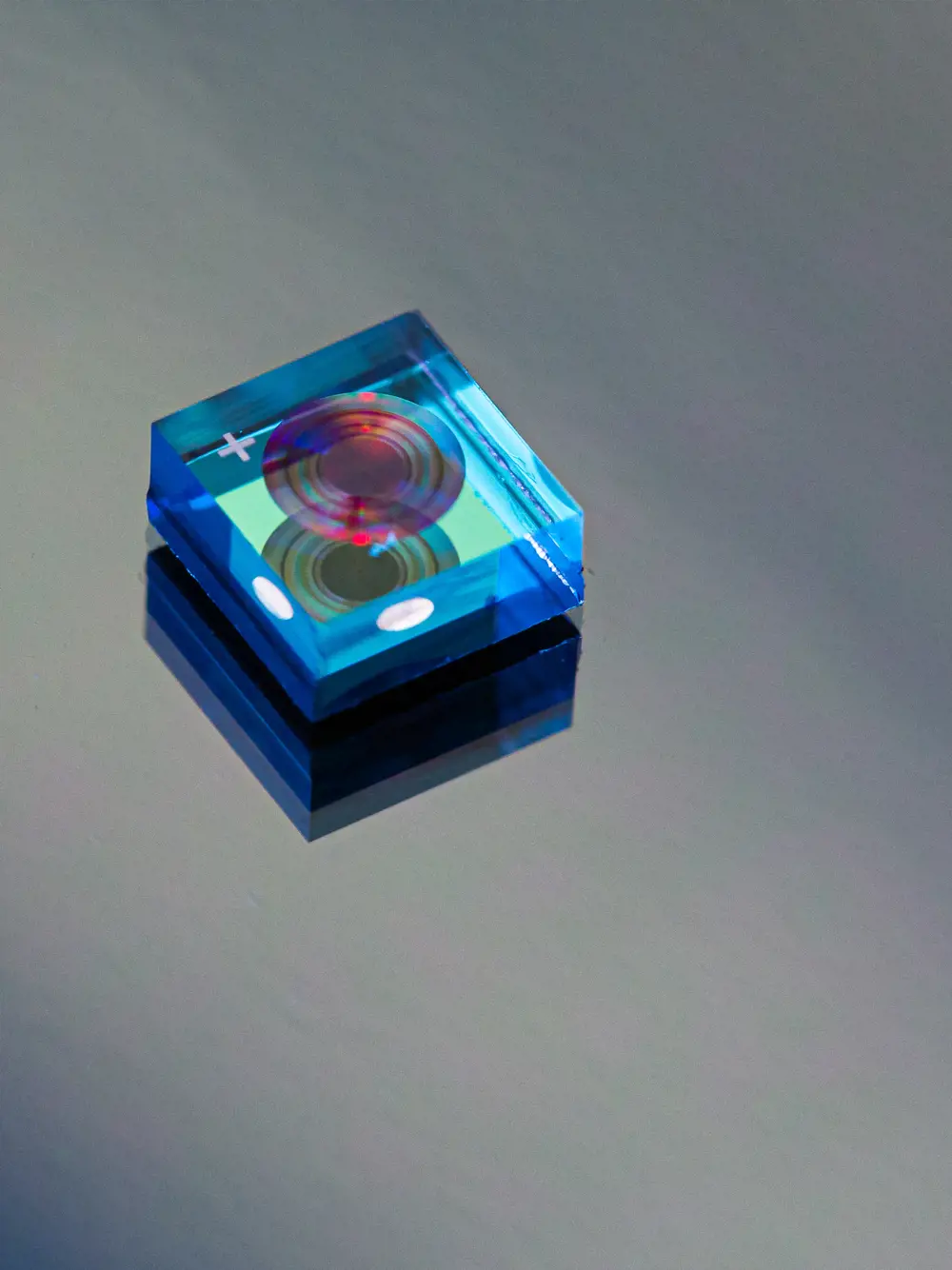
A single NIL Technology meta-optical lens, incorporated into a camera module © NIL Technology
What do metalenses mean for the future of diagnostics and VR?
The shared vision of thin smartphone cameras and their enormous market potential has accelerated the transition of metalenses from university labs towards mass manufacture. Startups such as Metalenz and NIL Technologies (NILT), large manufacturers such as STMicroelectronics, and major global consumer electronics companies such as Samsung are all working to drive the quality of metalenses up and their cost down.
Both Danish optics startup NILT and Harvard spinout Metalenz are on the cusp of mass production of their metalenses. NILT’s first commercially ready metalenses are targeted at 3D sensing for face identification and assisting autofocus in smartphones. Meanwhile, Metalenz is working with device manufacturers on 3D cameras for mobile devices and has said its lenses will be in consumer devices in 2022. The company has partnered with European semiconductor specialist STMicroelectronics to develop a manufacturing process for the lenses, and also plans to develop lenses for lightweight augmented and virtual reality systems.
This consumer technology focus is shared by NILT. “[Metalenses] have powerful capabilities beyond traditional optical lenses as they have completely flat surfaces, reduced thickness, and improved quality compared to classic refractive lenses,” explains Theodor Nielsen, NILT’s CEO and Founder. “They will be a game-changer for optical applications in consumer products, smartphones, and augmented, virtual and mixed reality devices.”
Beyond making smartphone cameras lighter, cheaper, and better, what about shrinking large scientific or medical imaging equipment down to a device that fits in the palm of the hand?
The growing industry traction in these areas is likely to act as a catalyst for the wider application of metalenses and metamaterials, resulting in new applications altogether. Beyond making smartphone cameras lighter, cheaper, and better, what about shrinking large scientific or medical imaging equipment down to a device that fits in the palm of the hand? Metalenz has said that with the right sensors, smartphones could identify specific molecules in blood for diagnostics, monitor air quality or tell whether a piece of fruit is ripe. Metalenses could improve LiDAR, robotic and machine vision, and even medical imaging, says NILT. Work from Harvard’s Capasso group (from which Metalenz spun out of) has suggested the possibility of turning a contact lens into a compound microscope. While we may not be there yet, it’s safe to say we’ve come a long way since Nero’s emerald.
***
This article has been adapted from "Metamaterials, Metalenses and Beyond", which originally appeared in the print edition of Ingenia 91 (June 2022).
Contributors
After studies in Aachen (Germany), Southampton (UK) and Socorro (US), he joined Southampton’s Optoelectronics Research Centre, where he has been leading research on metamaterials since 2010. He is a Marconi Young Scholar, Institute of Physics thesis prize recipient, and has been a Fulbright Scholar and Advanced Leverhulme Trust Fellow.
Keep up-to-date with Ingenia for free
SubscribeRelated content
Design & manufacturing

Super cool(er)
Welsh startup Sure Chill has developed a cooler that uses the properties of water to keep its contents cool for around 10 days without electricity. This is ideal for storing items such as vaccines where electricity sources are unreliable.

R&D investment makes good business sense
In just five years, Dr Ralf Speth FREng has presided over a revolution in design and manufacturing that has helped create a new family of engines and has overhauled Jaguar Land Rover (JLR) production facilities.

Steel can arise from the ashes of coal
Thousands of people were laid off in the UK steel industry in 2015 and there are pessimistic future forecasts. Professor Sridhar Seetharaman of the Warwick Manufacturing Group argues that smaller, flexible steel mills implementing new technology would better cope with fluctuating global trends.
Integrating metrology in business and academe
Professor Jane Jiang’s interest in measuring began when she worked on a bus production line in China. She found that the best way to improve quality, consistency and productivity was through metrology, the science of measurement. Today, she runs the UK’s largest metrology research group.
Other content from Ingenia
Quick read

- Environment & sustainability
- Opinion
A young engineer’s perspective on the good, the bad and the ugly of COP27

- Environment & sustainability
- Issue 95
How do we pay for net zero technologies?
Quick read

- Transport
- Mechanical
- How I got here
Electrifying trains and STEMAZING outreach

- Civil & structural
- Environment & sustainability
- Issue 95