Diamond technology: beyond hardness
In 2013, the world’s leading supplier of synthetic industrial diamond, Element Six (a reference to carbon, the sixth element of the periodic table), a De Beers Group Company, opened a £20 million Global Innovation Centre on the Harwell Campus, near Oxford. Home to over 140 material scientists, engineers and technicians, this facility is looking to progress development of both diamond-based abrasives and other technologies.
Shortly afterwards, a consortium of UK universities, led by Warwick, won £4.5 million of EPSRC funding – with more than £1.5 million more promised from industry – to establish the Centre of Doctoral Training in Diamond Science and Technology (DST). This centre aims to provide world-class training in cross-disciplinary materials and interfacial science, with a research focus on DST.
These properties enable [diamond] to outperform competitor materials in so many applications that synthetic diamond is now emerging as an engineering material
Natural diamond is a material known for its beauty and hardness. Historically, this led to its use in jewellery, where it is unsurpassed as the gem for all occasions. For over 60 years, industrial-grade diamond, usually produced by high-pressure high-temperature synthesis, has been utilised for cutting, grinding and shaping hard and abrasive materials. Today, this is a multi-billion pound business, and the challenges associated with the machining of many modern high-strength, lightweight materials have increased the demand for even tougher industrial diamond products.
More recently, advances in diamond synthesis have enabled the production of synthetic diamond in a variety of shapes and sizes, with properties other than hardness, such as high thermal conductivity, optical transmission and resistance to the effects of radiation, controlled and optimised – see Properties of synthetic diamond. These properties enable it to outperform competitor materials in so many applications that synthetic diamond is now emerging as an engineering material. Synthetic diamond can be used in many fields, including electronics, photonics, acoustics, pollution detection and quantum sensing and computing. It is currently applied in aerospace, construction, mining, healthcare and wastewater treatment. In all these, and many other activities and technologies, diamond is able to deliver solutions to previously unsolvable problems. Advances in synthesis and processing technologies are driving down the cost of synthetic diamond, which varies according to particle strength, size, shape, crystallinity, and the absence or presence of metal coatings. For many demanding applications, the cost is not prohibitive, and indeed, the performance gain makes it the material of choice. Many of these applications depend not only, or not at all, on diamond’s hardness. It is perhaps time to revise our view of synthetic diamonds: to look beyond hardness.
Properties of synthetic diamond
✨ From physical hardness, to electron mobility and resistance to radiation
- Exceptional physical hardness: 81 GPa
- Fracture toughness: 5.3 - 7 MPa m0.5
- Low thermal expansion coefficient: 1.1 ppm K-1
- Chemical and biochemical inertness: stable in most concentrated acids and alkalis
- Broad electromagnetic transmission spectrum: 225 nm to >50 μm
- Exceptional thermal conductivity: >20.0 Wcm-1K-1
- Excellent intrinsic electrical insulator: Resistivity ~ 1013 –1016 Ωcm
- Low dielectric constant: 5.7 at 35 GHz
- Low dielectric loss: <10-5 at 140 GHz
- Young’s modulus: 1,100 GPa
- Low coefficient of friction: Diamond on diamond clean surface μS ~ 0.1
- High acoustic velocity: 17,500 ms-1 at room temperature
- High resistance to thermal shock: >700 times higher than sapphire
- Wide electronic bandgap: - 5.5 eV
- Long-lived quantum states: T2 > 1 ms at room temperature (RT) for electron spin; T2 > 1 s at RT for nuclear spin
- Electrical conductor when suitably doped: Resistivity ~ 10-3 Ωcm
- High electron mobility: 2,200 cm2 V-1 s-1 at room temperature
- High resistance to radiation damage: Atom displacement energy Ed ~ 42 eV
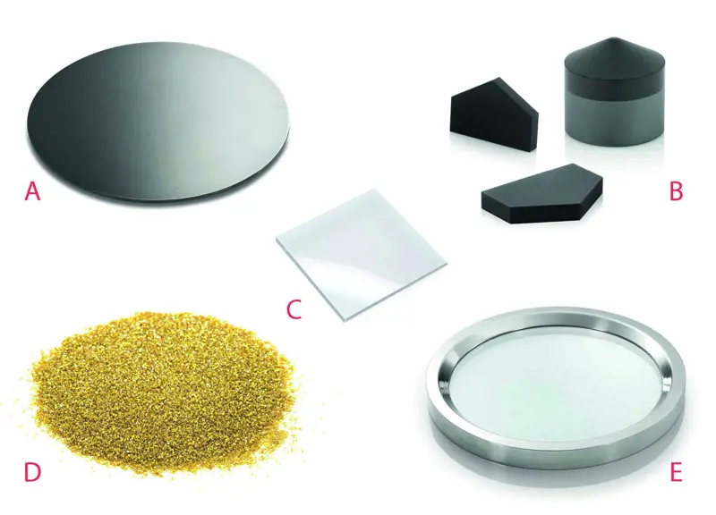
A range of synthetic diamond products grown by the high-pressure high-temperature and chemical vapour deposition (CVD) techniques. A: polycrystalline diamond disc (used in the precision machining of metals – up to 74 mm in diameter) B: polycrystalline diamond round tools (used in the machining of composite materials – up to 13.2 mm in diameter). C: CVD single crystal plate (used in spectroscopy – up to 8 x 8 x 2 mm) D: polycrystalline synthetic diamond grit (used in cutting and grinding tooling – up to 1,200 micron) E: polycrystalline CVD diamond window (used as an output window in high power CO2 lasers – up to 135 mm in diameter).
Abrasive uses
The hardness of diamond, its most evident property, was the first to be exploited by industry, and still underpins many of its most common uses. In wood and metal drilling and machining, in cutting stone and concrete, in grinding and polishing all manner of materials, in wire-drawing dies, in mining and tunnelling, and in oil and gas drilling, it boosts production and extends the useful life of tools.
The abbreviation PCD is widely used to describe a composite material that consists of micron-sized synthetic diamond powders bonded together by sintering at high pressures and temperatures. The varying orientation of the constituent micron-sized synthetic diamond grains provides a greater resistance to cleavage and is therefore a stronger material than single crystal diamond. PCD copes particularly well with the extreme conditions encountered in oil and gas drilling. In oil and gas production, demand for PCD drill bits is created by the industry’s need to work in ever more challenging circumstances. A well may have to be drilled to a depth of several miles. Currently, the only way to replace a worn or broken drill bit is to extract the drill string section by section: a long and consequently expensive process.
Moving from the previous industry standard, tungsten carbide, to PCD drill bits means more rapid drilling and fewer drill string extractions, providing substantial cost savings. In addition, diamond drills can tackle rock formations which tungsten carbide cannot drill into. In aggressive tests, PCD drill bits outlast tungsten carbide by more than a factor of a hundred. Over the last decade, the use of PCD as opposed to tungsten carbide has risen from 20% to more than 80% of the market.
The abbreviation PCD is widely used to describe a composite material that consists of micron-sized synthetic diamond powders bonded together by sintering at high pressures and temperatures
Making diamonds
💎 What are the different methods to make diamonds?
Natural diamond is the product of carbon-bearing materials that have been subjected to high pressure, and to temperatures of 900 to 1,300°C deep (~100-200km) in the Earth’s mantle. Diamond is produced in a thermodynamically stable environment from a surrounding carbon-rich melt.
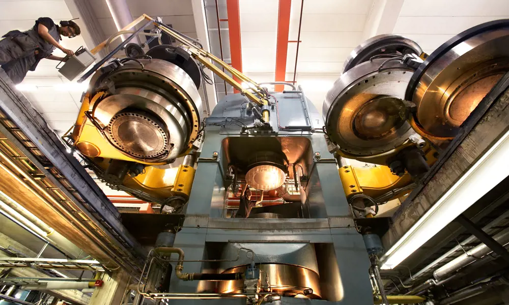
In contrast to its natural genesis, the presence of a solvent metal, such as iron, cobalt or nickel has been found necessary for a practical, consistent, industrial high-pressure high-temperature (HPHT) method of diamond synthesis. At high temperatures (typically 1,300-1,500 °C), carbon atoms (from, for example, a graphite source) are dissolved in the molten metal. At extremely high pressures (typically 50,000-60,000 times atmospheric pressure), diamond is the stable form of carbon. By controlling HPHT conditions, micrometre-sized diamonds can be rapidly (in minutes) produced for abrasive applications. The pressure is the equivalent of placing the Eiffel Tower on top of a drinks can. These types of HPHT-produced diamond have been manufactured commercially since the 1950s.
By employing a diamond seed – a small crystal of natural or synthetic diamond – and controlling the temperature gradient inside the HPHT capsule, carbon atoms can be deposited on this seed to produce larger single crystals of diamond (dimensions >10 mm are possible). In the HPHT process, it is hard to control the uptake of impurities, and the size of the diamonds produced is limited by the size of the HPHT cell.
A more recent alternative to HPHT, available since the early 1990s, is the chemical vapour deposition (CVD) method. It utilises a gas, typically methane (CH₄), as a carbon source and hydrogen (other gases can be added to influence the chemistry). Carbon can then be deposited onto a suitably positioned substrate. Under the conditions used for CVD diamond synthesis, graphite is the thermodynamically favoured phase of bulk carbon (that is to say most energetically stable phase) rather than diamond. Hydrogen radicals are able to etch away any graphite that forms on the substrate far faster than they can remove any diamond. The kinetics of the processes at the surface enable diamond to be the only form of carbon left at the end of a synthesis run.
Diamond grown by CVD can fall into three categories – nanocrystalline, polycrystalline and single crystal. Nanocrystalline diamond refers to isolated crystals or continuous films where the individual diamond crystals are typically smaller than 500 nanometres in any one direction. Polycrystalline CVD diamond refers to continuous films made up of interlocking diamond crystals typically larger than one micron. Nanocrystalline and polycrystalline diamond is typically formed whenever growth occurs on a non-diamond substrate. Nanocrystalline diamond films do not have all the unique properties of diamond, but there is a range of interesting applications in tribology, micromechanics and biochemical sensing. Large-area wafers (typically 15 cm in diameter) of thick (several mm) polycrystalline diamond can be produced by the CVD process. Single crystal diamond is formed by homoepitaxial growth (growth extending outwards from the surface of a crystal in all dimensions), where the seed, or substrate, is a single crystal diamond.
The global output of industrial diamonds is now around 1,000 tonnes a year. Most of this diamond is synthesised for its abrasive properties and is made using the HPHT method. Diamond produced for other purposes, especially for many of its high-tech applications, is primarily grown using CVD. CVD diamond forms around 0.1% of all synthetic diamond production.
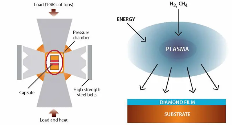
Left: Schematic of high-pressure high-temperature (HPHT) belt press for the synthesis of diamond.The upper and lower anvils supply the pressure load to a cylindrical inner cell. This internal pressure is confined radially by a belt supporting the carbide die. Electrical current is used to heat the capsule, which contains the carbon source and the solvent metal; under HPHT conditions, the carbon is dissolved in the molten metal and crystallised out as diamond.
Right: Chemical vapour deposition: inside a reaction chamber, at or below atmospheric pressure, a mixture of methane (CH₄) and hydrogen is activated by a hot filament or a plasma to dissociate the methane and hydrogen source gases. Carbon can then be deposited on the substrate atom by atom. The additional hydrogen in the chamber is there to terminate the dangling carbon bonds of the carbon atoms as the diamond lattice grows; this stabilises the surface of the crystal and prevents it from reconstructing into a non-diamond form. CVD diamond synthesis could not happen without this hydrogen
Diamond even finds a place in road mending where surface layers of asphalt or concrete need to be removed, with PCD picks providing over 40 times the life of standard road pick material.
The demand for diamond as a material with abrasive properties is well established. In practice, there are still advances to be made. Some of these are simply to improve its performance. The engineering involved here is not only that of increasing the toughness of the diamonds themselves; the sintering process by which they are bonded to the matrix holding them firmly in the tip of the bit is just as important. And the science of sintering is equally complex.
A more predictable driver of the advance of diamond for abrasive purposes is materials science, which grows increasingly ingenious in devising novel materials with new properties
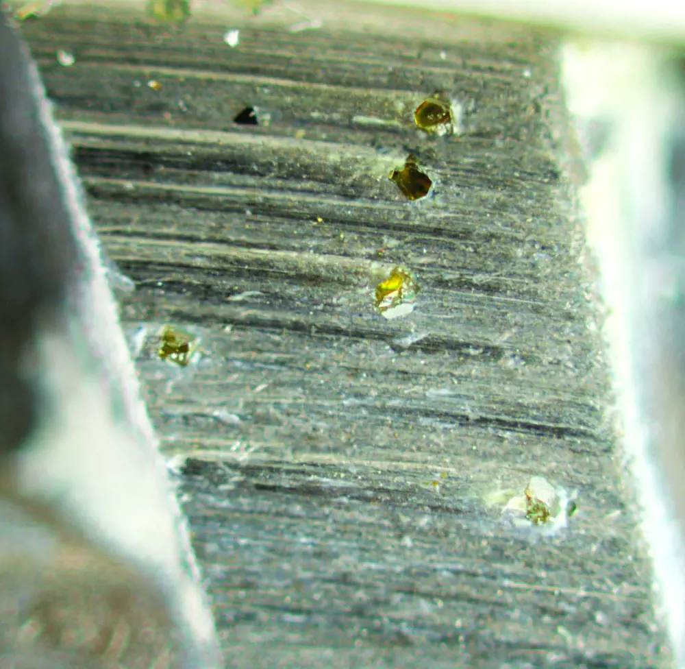
Diamonds in an angle grinder blade © Hustvedt
A more predictable driver of the advance of diamond for abrasive purposes is materials science, which grows increasingly ingenious in devising novel materials with new properties. Any material developed to meet extreme challenges is likely to be more difficult to machine. Carbon fibre reinforced polymer (CFRP), for example, is now increasingly popular, in particular with the aerospace industry. Conventional tools wear rapidly in drilling and milling CFRP, and cause delamination between the fibre layers. Diamond copes more successfully. Moreover, new materials of this kind are constantly evolving, and tools that can successfully drill or cut one generation are not always well-suited to coping with the next. Today’s innovation in materials science prompts tomorrow’s innovation in the technology of abrasion, including the development of new forms of diamond tooling.
In addition to these demanding industrial and engineering applications, diamond finds roles in the most delicate of work. Single crystal synthetic diamond can be manufactured with an ultra-fine cutting edge ideal for use in the most delicate surgical operations from ophthalmology to neurosurgery.
Optical uses
One of diamond’s key advantages is that it has a broad transmission spectrum running from 220 nm to >50 microns, covering the ultraviolet, the visible, the far infrared and the microwave regions of the electromagnetic spectrum. Needless to say, anyone in possession of an optically perfect natural diamond one or two centimetres in diameter would sell it on the gem market, not hand it to a scientist for slicing up and fitting into a piece of scientific apparatus! However, the advent of techniques for growing high quality synthetic diamond in thin plates has made optical applications a practical possibility.
Diamond has found applications in spectroscopy, high-power radiofrequency generators, long wavelength infrared imaging, disc lasers, Raman lasers and high-power CO2 lasers. Its role in the last of these illustrates why diamond is so valuable. To make practical use of the output of a high-power CO2 laser (used, for example, for laser cutting and welding of steel), the radiation beam it generates has to be able to escape the chamber in which the lasing gas is confined. This it does through a window at one end of the laser’s casing. But if too much of the emerging beam is absorbed on passing through the window, this can lead to overheating and the formation of a thermal lens, which strongly affects the beam quality and the position of the laser focus.
Before diamond, the output power of such lasers was limited by the material properties of the window. Because of its high thermal conductivity, low variation of refractive index with temperature and excellent infrared transparency, diamond can handle much higher power levels than competitor window materials without any deteriorating effect on the laser beam.
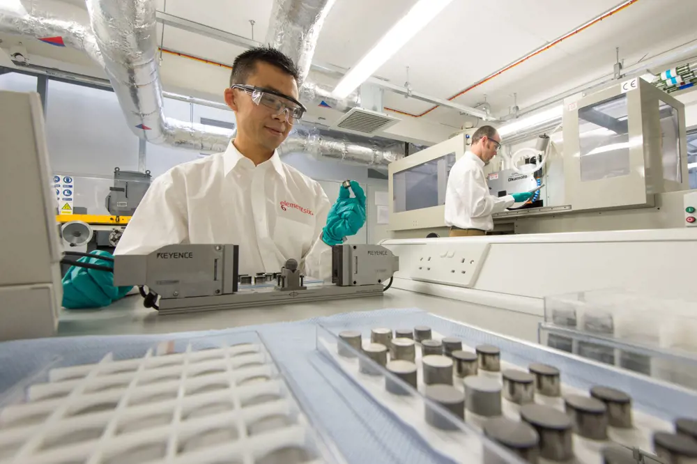
Synthetic diamond oil and gas cutters under analysis at Element Six’s Global Innovation Centre. The engineer is holding a cylinder manufactured by sintering diamond powder (at high temperature and pressure) on a tungsten carbide substrate. Many such disks are mounted in a drill bit (the teeth) for drilling through rock © Element Six
The development of low absorption and low birefringence (whereby the refractive index depends on the polarisation and propagation direction of light) CVD diamond with excellent thermal properties has enabled significant improvements in the performance of both doped dielectric and semiconductor disk lasers. Perfect diamond is optically isotropic, and the occurrence of birefringence is a result of the photoelastic effect: the change of refractive index caused by strain originating from defects such as dislocations. Pure natural diamonds free from birefringence are very rare, and it is challenging to produce such material in the laboratory. Diamond heat spreaders bonded to the pumped surface of doped dielectric gain crystals allow higher pump power densities to be employed, and allow a level of output that would otherwise cause the laser crystals to fracture. Intracavity diamond heat spreaders have also proven vital for semiconductor disk lasers at watt-level powers.
Another area of recent development is the use of diamond in Raman lasers. Here, diamond is used as the active laser medium – the incident pump light is Raman-scattered to a new wavelength, whereby this scattered light is amplified by the third-order nonlinear optical process of stimulated Raman scattering. Diamond offers the largest wavelength shift – for example from 532 to 573 nm. Couple this with its exceptional thermal conductivity and the production of high power (Raman) lasers at hitherto inaccessible wavelengths is possible.
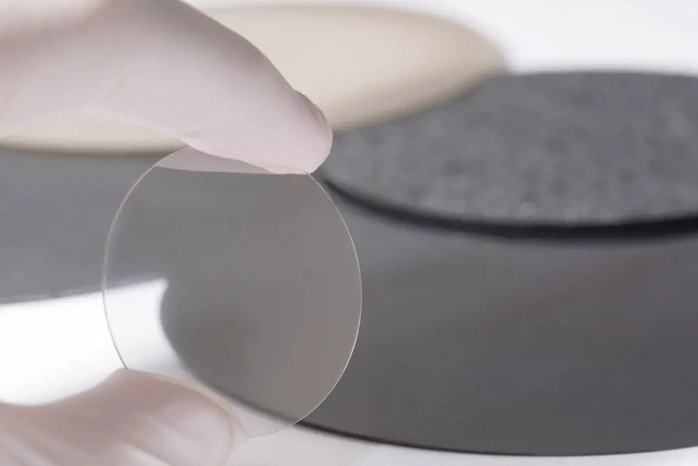
A transparent 25 mm-diameter polycrystalline diamond window produced by chemical vapour deposition (CVD) suitable for infrared laser and other optical applications. In the background are large dark mechanical grade wafers of diamond produced by CVD © Element Six
Sound and fury
While diamond’s value in optics makes clear sense, its role in acoustics is less intuitively obvious. The property of value here is its mechanical stiffness. Being light, but very strong, means that its specific stiffness is among the highest of any material. In good quality acoustic systems, a speaker diaphragm may have to vibrate very quickly – perhaps at 20,000 Hz. What is needed is a diaphragm that moves the air, but without flexing and so adding its own ‘colour’ to the sound. Diamond provides this. It is possible to manufacture a cone-shaped component that is two or more centimetres in radius at the base, and some 40 microns thick (a human hair has a diameter of 30-100 microns). In 2012, Element Six and Bowers and Wilkins were jointly awarded the Queen’s Award for Enterprise in Innovation for the development of the synthetic diamond tweeter dome.
Diamond also excels in radiation detection applications where volume sensitivity, radiation hardness and/or temperature insensitivity are required.
Diamond also excels in radiation detection applications where volume sensitivity, radiation hardness and/or temperature insensitivity are required
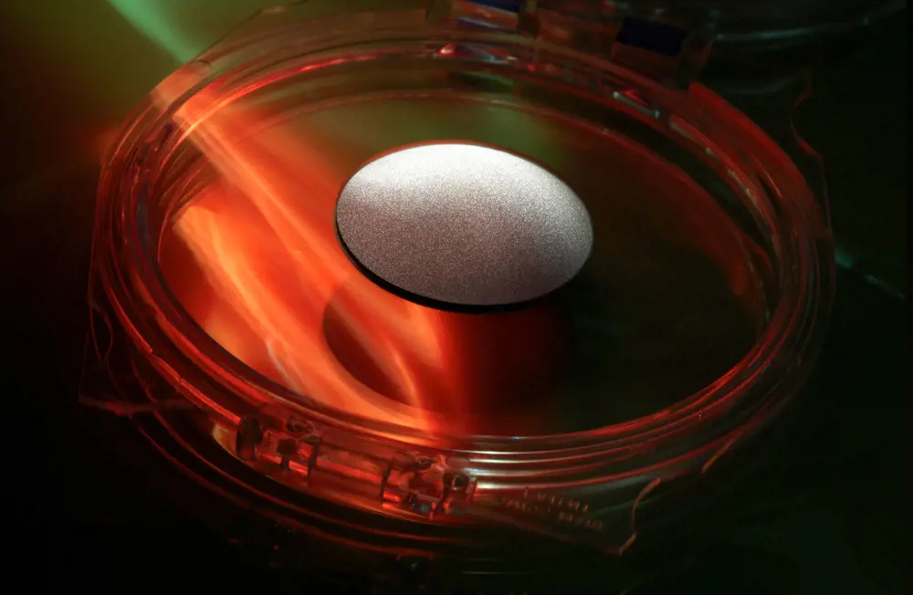
An unmounted synthetic diamond tweeter dome approximately 25 mm across (manufactured by Element Six) sitting in a membrane box and used in Bowers & Wilkins speakers © Element Six
High-purity intrinsic diamond is able to act as a solid state ionisation chamber at room temperature, and although there are other diamond-detector modalities, this is the one most commonly exploited. The transit of high-energy charged particles through the diamond leaves behind it a trail of excited/ionized atoms and electron-hole pairs. When a voltage is applied across the diamond, the electrons and holes move away from one another in the electric field, generating an electrical signal in an external circuit. Charge must be able to travel freely through the lattice, so the key to good performance is the purity and crystalline quality. Diamond’s radiation hardness arises from its high atomic displacement energy (42 eV/atom – the covalent bonds across the lattice structure are very strong) and low atomic number. For high-energy particles, diamond is an order of magnitude more radiation-hard than silicon.
The Large Hadron Collider and the ATLAS Beam Condition Monitoring System in use at CERN during its search for evidence of the Higgs Boson both utilised synthetic diamond detectors. The experiments carried out at CERN have been designed to track and characterise the output of particle collisions inside the machine. The beams used to generate these collisions are highly energetic and damage most materials, and around the collision site there is a great deal of radiation. Using synthetic diamond detectors meant that the monitoring systems were able to withstand these conditions.
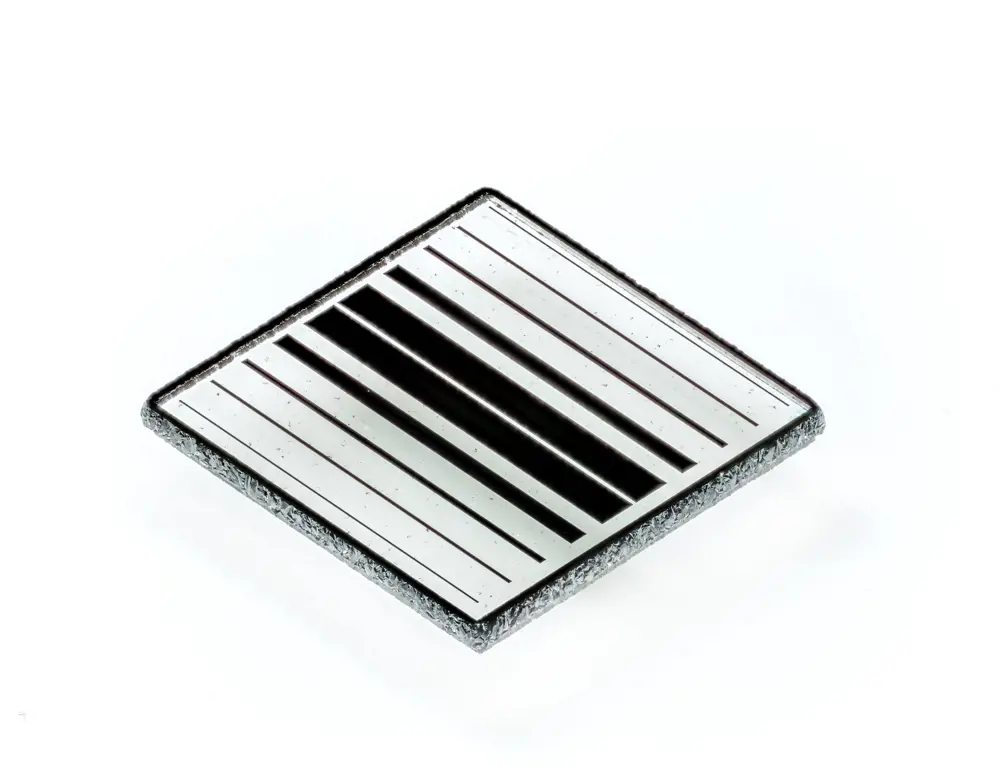
An intrinsic piece of polycrystalline CVD diamond (colourless) into which has been grown borondoped electrically conducting diamond bands of different widths. The chemical resistance of the all-diamond device means that the conducting diamond band electrodes can be used as sensors, even in highly corrosive environments Picture taken by Dr Jon Newland; device fabricated by Element Six Ltd and the University of Warwick
Conducting properties
Pure (intrinsic) diamond is an excellent electrical insulator. However, if, during its manufacturing process, it is doped with sufficient boron atoms (replacing approximately one in 1,000 carbon atoms), then it becomes a respectable electrical conductor with a resistivity of ~10-3 Ωcm. One of the more ingenious methods of exploiting diamond’s conducting properties is in the treatment of waste water contaminated with anything from dyes to sewage. Being chemically inert, a conducting diamond can constitute a non-corroding electrode. When used to pass a current through an aqueous fluid, it can generate reactive radicals such as peroxide and hydroxyl: oxidants able to attack a variety of pollutants, both organic and inorganic. This breaks pollutants down into harmless salts and carbon dioxide, avoiding the need to add any further chemicals. Diamond electrode devices have been proposed for the disinfection of drinking water, swimming pool water and industrial cooling water.
Another application of conducting diamond is as an electrode for chemical sensing and for performing analytical chemistry. Diamond has found a variety of uses from detecting heavy metals in sea water to the study of brain biochemistry. Because their material is so chemically inert, diamond electrode sensors suffer no damage in even the most hostile environments. Conversely, their inertness and biocompatibility mean that they create no threat of contaminating any environment into which they are introduced – particularly valuable when contemplating their use inside the human body.
The effectiveness of diamond as a heat spreader in electronic packages depends very much on how it is integrated into the module, and its optimal application is a hot (pun intended!) research topic at the moment
Although active diamond electronic devices are a long way off, diamond is establishing a rapidly developing role in electronics. Besides being an electrical insulator, it is also a good conductor of heat – five times better than copper. This is important in the thermal management of electronic devices and tiny or delicate circuits that may generate large amounts of heat in a small space with destructive consequences. This thermal challenge is at the forefront of designers’ minds as they struggle to design packages for circuitry; more than half of failures in today’s electronic systems are a result of excessive temperature rises, and this trend is only going to get worse. The effectiveness of diamond as a heat spreader in electronic packages depends very much on how it is integrated into the module, and its optimal application is a hot (pun intended!) research topic at the moment.
Quantum technologies
A much-discussed, though as yet unrealised, role for diamond will lie in a range of quantum technologies including cryptography, computing and sensing. Although the first two of these applications may be several years away from becoming practical reality, quantum sensors (operational at room temperature) utilising the negatively charged nitrogen-vacancy colour centre to measure, for example, weak magnetic fields (magnetic resonance imaging on the nm scale) or the local temperature within a cell, have been demonstrated in the laboratory. With diamond-based quantum technologies, physiology could become a science practised not just at the level of organs and tissues but at the cellular and even sub-cellular level.
The specific value of diamond in quantum technology will no doubt be boosted by a new £270 million government investment in a National Quantum Technologies Programme. Managed by EPSRC and Innovate UK, it has established a network of four quantum technologies hubs led by the universities of Birmingham, Glasgow, Oxford and York. Working in partnerships with industry, these hubs will focus on transferring basic quantum science out of the laboratory and establishing a new quantum based industry in the UK.
Multifaceted
Element Six is a global company at the forefront of the rapid development now taking place in diamond technology. Its new global innovation centre (GIC) near Oxford, which opened two years ago, has manufacturing, analytical and testing facilities that allow potential new applications to be taken from the ideas stage through to the point at which novel diamond products are suitable for commercial manufacturing.
Much of the research at the GIC is focused on designing and testing new materials for cutting and grinding applications. More technical applications, addressed using CVD diamond, include engineered optical components for lasers, fusion reactors and semiconductor lithography, thermal management materials and structures for electronic devices such as are used in the mobile phone industry. GIC also looks at the nanoscale engineering of diamond defects responsible for the important quantum properties that will enable quantum technologies to become a reality.
as it becomes increasingly clear just how far the properties of diamond extend beyond hardness, it looks as if diamond is beginning to resemble the ultimate engineering material
Academic interest in diamond is also on the rise, as evidenced by the recent creation of the EPSRC’s Centre for Doctoral Training in Diamond Science and Technology based at the University of Warwick. The centre has set up a consortium of eight universities – Warwick, Aberystwyth, Bristol, Cardiff, Imperial, Newcastle, Oxford, and Strathclyde and 40 academic partners to unite the UK diamond community under one umbrella, to provide excellence in graduate training and research, sharing resources and pooling expertise. The centre also strives to develop and foster collaborative links with industry and enable efficient technology transfer.
Indeed, as it becomes increasingly clear just how far the properties of diamond extend beyond hardness, it looks as if diamond is beginning to resemble the ultimate engineering material.
***
The author would like to thank Geoff Watts, science and medical writer, for his help in the preparation of this article. Watts interviewed Dr Richard Bodkin, principal research scientist at Element Six's Global Innovation Centre (GIC) and Dr Geoff Scarsbrook, Technologies R&D Manager at GIC.
This article has been adapted from "Diamond technology: beyond hardness", which originally appeared in the print edition of Ingenia 63 (June 2015).
Contributors
Mark Newton is a Professor of Experimental Physics at the University of Warwick. His research focuses on the structures and properties of defects in diamond and the development of diamond-based sensor technologies. The sensor activities focus on the exploitation of the spin and optical properties of colour centres in diamond and the development of novel spectro-electrochemical devices.
Keep up-to-date with Ingenia for free
SubscribeRelated content
Materials

Aerogels
Among some of the lightest known solid materials, aerogels, formed by removing liquid from gels, have many uses ranging from catalysts and sensors, to being used on NASA missions.

Recycling household waste
The percentage of waste recycled in the UK has risen rapidly over the past 20 years, thanks to breakthroughs in the way waste is processed. Find out about what happens to household waste and recent technological developments in the UK.
A lot more than lubrication
The control of friction and wear in mechanical systems by lubrication and surface engineering has led to safer, faster transport as well as medical innovations. Ian Hutchings FREng, GKN Professor of Manufacturing Engineering at the University of Cambridge, highlights the progress and some failures of the important discipline of tribology.

Toughened glass
A stronger version of standard glass, toughened glass is ideal for use where greater strength or safety is needed. Learn how thermal and chemical treatments enhance strength, safety and durability for various applications.
Other content from Ingenia
Quick read

- Environment & sustainability
- Opinion
A young engineer’s perspective on the good, the bad and the ugly of COP27

- Environment & sustainability
- Issue 95
How do we pay for net zero technologies?
Quick read

- Transport
- Mechanical
- How I got here
Electrifying trains and STEMAZING outreach

- Civil & structural
- Environment & sustainability
- Issue 95